Experts estimate that the global market for silicon wafers will reach $16.01 billion by 2028. This goes to show just how important these components are to the global economy. They are primarily used in semiconductor manufacturing and manufacturers place semiconductors in thousands of electronic devices.
Despite the high demand, the process of creating silicon wafers has remained precise. Any defects in wafers can affect how well electronic devices perform. They must be perfect.
The wafer polishing process upholds these expectations. Read on to learn more about the steps for polishing silicon wafers.
Why Is Wafer Polishing Necessary?
Silicon wafers must have certain depths for specific applications. They must also have no imperfections. Getting these factors wrong can negatively affect a final product.
Polishing gets rid of imperfections and flattens silicon wafers. It also makes manufacturing less costly and more efficient.
Methods of Polishing Silicon Wafers
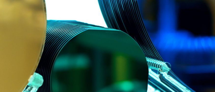
Manufacturers can polish one or both sides of silicon wafers. Which method they decide to go with depends on the final application of each silicon wafer.
To polish the wafers, manufacturers usually use the Chemical Mechanical Wafer Polishing (CMP) process. This process is also often known as Chemical Mechanical Planarization.
Chemical Mechanical Wafer Polishing (CMP)
The CMP process involves chemicals and mechanical polishing. One purpose of this is to remove materials from the wafer surface. If materials remain, they can affect how well the final product performs.
Another purpose is to make the silicon wafer surface uniform. It will remove any irregular bumps, divots, etc. on the silicon surface. A flat silicon wafer will fit more easily into its target electronic device.
Slurry
A manufacturer uses an abrasive and corrosive chemical slurry in the CMP process. The type of slurry they use depends on the particular application. Different chemical slurries cause different rates of material removal.
Polishing Pad
A mechanical device will drip the chemical slurry onto a polishing pad. The diameter of the polishing pad is usually much longer than that of the silicon wafer. There are a variety of polishing pads workers may use that can change the rate of material removal.
Polishing Head
A dynamic polishing head holds a wafer in place. The target surface of the wafer faces the slurry-covered polishing pad.
Between the dynamic head and the silicon wafer will be a substrate known as a carrier wafer. Workers often bond this to the silicon wafer to protect it.
Rotation
The head spins the wafer and moves it back and forth across the polishing pad. The polishing pad also rotates. More chemical slurry gets added to the polishing pad as the polishing process continues.
CMP Test Wafers
Without Chemical Mechanical Wafer Polishing, there are no polished silicon wafers. If electronic devices do not have polished wafers, they would work extremely poorly. Let's thank all the innovators who brought about the CMP process.
Do you need test wafers for your CMP process? If so, we at Silyb Wafer Services can help you. We create our patterned short-loop designs using industry input.
Request information about some of our custom test wafers on this page.
Published June 21, 2023.