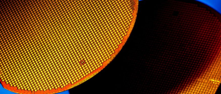
Integrated circuit (IC) fabrication is a complex process involving the use of silicon and precise methodologies to create intricate semiconductor components. Test wafers serve a crucial function in this process, undergoing extensive wafer testing comparable to a final product assessment. By identifying potential issues early in the process, test wafers facilitate flawless production of semiconductor devices.
Role of Test Wafers in IC Fabrication
Test wafers are used for the early detection of flaws, such as short circuits or malfunctioning transistors. These wafers are identical to the actual wafers used in the fabrication process, except that they will not be processed into final products. Instead, they are used to run tests that can identify potential issues that might affect the quality and functionality of the ICs to be produced.
Identifying Defects and Potential Issues
Before the actual wafer production begins, test wafers undergo various tests that evaluate if they meet the desired quality and performance standards. These tests uncover defects such as short circuits, malfunctioning transistors, and other potential issues that might impact the final products. Test wafers serve as a blueprint, enabling engineers to identify problem areas and fine-tune the fabrication process accordingly, without having to deal with the consequences of a failed batch.
Reducing Costs and Minimizing Waste
The financial implications of identifying defects early in the IC fabrication process are significant. A single faulty IC can not only compromise the functionality of the entire wafer but also result in a substantial loss of production time and resources. By using test wafers to identify and address defects in the early stages, manufacturers minimize the risk of producing faulty ICs and can focus on optimizing the fabrication process, resulting in cost savings and reduced waste.
The Changing Landscape of Wafer Testing Methods
Traditional wafer testing methods were straightforward—engineers were mainly concerned about whether the chip could power on. With the rapid evolution of semiconductor complexity, wafer testing methods evolved, leaning towards a mix of functional and reliability tests to affirm that each silicon wafer can fulfill modern technological demands.
Electrical and Optical Testing Techniques
The goal is to consolidate all silicon wafers to zero defects. Achieving this requires going beyond electrical connectivity checks; IC fabrication efficiency is boosted when traditional electrical testing is combined with optical inspections to identify elusive defects unnoticeable through mere voltage checks.
Artificial intelligence (AI) has emerged as a key player in this realm. The incorporation of AI in wafer testing mimics the fusion of Sherlock Holmes and Iron Man, with advanced tools spotting microscopic clues and potential yield-impacting defects before they escalate to significant problems. It enhances the efficiency of IC fabrication test wafers by addressing defects with an accuracy that the human eye might miss, thereby fostering high-quality ICs.
Efficiency and Cost-Effectiveness
The use of test wafers allows for constant monitoring and optimization of the IC fabrication process. The data gathered from wafer tests offers valuable insights for process tweaking, and equipment tuning, and it can guide decisions for setting production parameters. The automation of these tests further contributes to making the production process more efficient by reducing timescales and human error.
The financial implications of inefficient IC fabrication processes can be severe. Given the high cost of semiconductor materials and the complexity of the manufacturing steps involved, early fault detection is essential to maintain the economic viability of IC fabrication. Thus, test wafers provide a cost-effective method for fault detection and process optimization, directly impacting manufacturing efficiency.
Advanced Techniques in Semiconductor Device Testing
Equipment crucial for IC fabrication testing has adapted to suit the fluidity of ever-evolving semiconductors. The contribution of automated test equipment (ATE), an orchestra conductor of the IC fabrication world, is integral. It sees to it that each semiconductor instrument strikes the correct note, thereby promoting the production of streamlined and precise chips.
Probe cards, a pivotal component of ATE, make precise micro-connections to the tiny bond pads on a single wafer. Their ability to adapt and evolve mirrors the dynamic nature of technology itself.
Just as each medical diagnostic tool serves a unique purpose, different testing techniques spotlight unique aspects of device performance. Radiofrequency (RF) probing delves into high-frequency device behaviors, while Direct Current (DC) probing provides precision for low-frequency or static measurements. Parametric probing, on the other hand, provides valuable data points for optimizing silicon die performance. These diverse testing tools reflect practical necessity, stressing the importance of smarter methods to test smart chips, enhancing IC fabrication efficiency.
Wafer Probing and Quality Control
In semiconductor manufacturing, wafer probing reinforces quality control. Every semiconductor die is meticulously scrutinized under high-stress conditions to detect anomalies like short circuits. With accurate measurement through wafer probing, manufacturers can maintain high yields and save significant costs down the line.
Wafer probing provides valuable feedback that manufacturers use to fine-tune fabrication methods—another essential step to ensuring each silicon slice meets the required standards. By catching these issues early on, wafer probing prevents the catastrophe of scrapping an entire batch due to a faulty electrical contact—promoting efficiency and cost savings.
Navigating Challenges in IC Fabrication Testing
IC fabrication testing presents a high-stake challenge. Manufacturers face not only monetary consequences when an issue is overlooked but also risk slipping behind in an intensely competitive semiconductor industry.
Efficient process control has evolved to manage high-temperature fluctuations during wafer tests. In the same vein, strategies to deal with sneaky issues like short circuits have taken the foreground. Early detection of imperfections prevents drastic issues akin to catching a cold before it turns into pneumonia. Vigilance in IC fabrication testing results in smooth production and maximum efficiency.
In conclusion, the role of test wafers cannot be overstated in IC fabrication efficiency. They facilitate proactive problem-solving, enhance quality control, and drive improvements in the production process — all leading to optimized fabrication efficiency.
Published February 19, 2024.