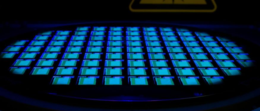
Did you know that the digital devices you're using right now owe their existence to something called "wafer lithography"? We're talking about your smartphones, computers, and tablets.
It's a mind-boggling concept, isn't it? That's right; this intricate, highly technical process is the backbone of modern digital technology. It may sound like something from a science fiction novel, but it's a very real and incredibly essential part of our everyday lives.
There's the smooth operation of your favorite app to the precision control of advanced machinery. These tiny patterns are etched into silicon wafers through lithography making it all possible.
Let's look into this matter a little more.
Getting to Know the Key Player: The Silicon Wafer
Wafer lithography starts with a player you might not expect: the humble silicon wafer. This simple, shiny disc is the canvas where the entire magic happens. So, how do we get there?
Before we dive into the lithography silicon wafer process, let's take a quick peek at what a silicon wafer is. In essence, it's a thin slice of semiconductor material, often silicon, used as the substrate for integrated circuits.
The wafer provides the base where the magic of patterning happens. Think of it like the plain, white piece of paper before a masterpiece is drawn.
Understanding the Wafer Lithography Process
So, how does this wafer lithography process work? Let's break it down together.
At its core, wafer lithography is the process that patterns wafers to create semiconductor devices. It's like an intricate dance; each step is precisely choreographed to achieve perfection.
First, a layer of photosensitive material is spread across the wafer. It's then baked to harden. After this, a mask is used to project an intense beam of light onto the wafer. This light is where the name "optical lithography" comes from.
The light causes the photosensitive material to become soluble, so when it's washed, a pattern emerges. After a few more steps, such as etching and removal of the mask, we're left with the patterned wafer, ready for use in devices.
Why Pattern Wafers? The Importance in CMP Tests
Now, you might be wondering, "Why do we need to pattern wafers?" Here's why.
Pattern wafers are the workhorses in CMP tests. CMP stands for Chemical Mechanical Planarization. This process is used to smooth surfaces on wafers, and the pattern helps in evaluating the efficiency and accuracy of this smoothing process.
CMP tests use a pattern wafer and a blank or test wafer. By comparing the results on both, experts can determine if the process has worked correctly. It's like a control and experimental setup in a science experiment!
Getting Your Hands on Wafer Solutions
If you're in the market for patterned wafers for CMP or any other semiconductor application, there are numerous wafer solutions available. Depending on your needs, you can get wafers with different diameters, materials, and patterns.
Remember, when choosing your wafer solutions, consider the applications you'll be using them for. Test wafers, for instance, should be appropriate for the specific test you're conducting.
The Marvel of Wafer Lithography
Wafer lithography, then, is not just a process. It's an art; a marvel that underpins our digital world. As we continue to advance technologically, this intricate dance of light, chemicals, and silicon will continue to hold center stage, etching our future in the clean rooms of wafer factories around the world.
Here you can see some examples of cutting-edge patterned silicon wafers at 200mm CU.
Published August 21, 2023.
