Is your semiconductor manufacturing company creating more wafers than ever in 2023? You're in good company.
Research shows the semiconductor wafer market worldwide in 2021 was worth more than $11 billion. It's anticipated to grow more than 6% by 2030, reaching $15 billion. A major reason for this is the increasing demand for wafers in the cloud computing industry.
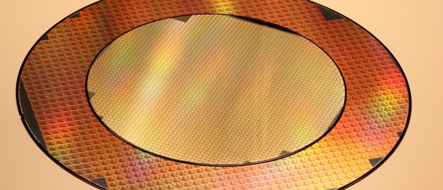
A patterned silicon wafer may help you stay ahead of your competition in the semiconductor industry. What is a patterned wafer? Why do you need a patterned silicon test wafer?
What types of silicon wafers exist? What are the main applications of silicon wafers? Let's explore the ins and outs of patterned wafers.
Patterned Wafer: What Is It?
A patterned wafer is a thin disc used for manufacturing an integrated circuit, also known as a microchip. Integrated circuits feature several interconnected, small components used in today's electronic devices. These include resistors and transistors.
Resistors block electrical currents from flowing in electronic circuits. Transistors increase electronic signals.
A special process is used to create the pattern found on a patterned wafer. The patterning process involves applying a layer of silicon to the wafer.
The layer is then exposed to light. Any exposed area is etched away.
This process must be repeated multiple times. All layers are eventually etched based on the design requirements (more on the wafer fabrication process later).
The patterning procedure requires expertise and precision. This is why many semiconductor manufacturing firms outsource it.
Patterned wafers are similar to standard wafers because both types of silicon wafers are clean and high-quality. A patterned wafer is more reliable and uniform, though. This makes it a better option for manufacturing and engineering.
Patterned Wafer Importance
Society needs faster processors to accommodate modern technology's advances. This means the space on chips must be used more efficiently.
More features have to be packed into smaller areas while maintaining strong performance levels. This is where a patterned silicon wafer comes into play.
These types of silicon wafers can help you create smaller chips more quickly. That's because they're more dependable and consistent as we mentioned earlier.
Types of Silicon Wafers
Two main types of silicon wafers exist: doped and undoped silicon wafers. Let's go over these two types of wafers.
Doped Wafers
A doped wafer is created by introducing a dopant, or a certain impurity, into the wafer's silicon crystal. These impurities may include chemical elements such as boron, phosphorus, antimony, and arsenic.
Adding boron to the wafer's silicon produces a P-type wafter. This type of wafer has several holes with positive charges.
Antimony, arsenic, and phosphorus may be added to wafers' silicon to produce N-type wafers. These types of wafers feature negatively-charged electrons.
Some doped wafers are degenerate, and others are extrinsic. Degenerate wafers have large concentrations of dopants. Extrinsic ones have moderate or small amounts of dopants.
Undoped Wafers
An undoped wafer doesn't contain dopants. This type of wafer may also be called a float zone or intrinsic zone. It features crystalline silicon only.
Doped wafers have a couple of advantages over undoped ones. A doped wafer is more efficient in a semiconductor since it has greater electrical conductivity. It's also easier to manage.
Patterned Wafer Fabrication
A patterned silicon wafer is created using a process known as photolithography. The process involves developing patterns on a wafer's surface using light as we mentioned earlier. It must be performed in clean room environments to protect the wafer from contamination by particles, like dust.
The first step wafer fabrication step is to coat a silicon wafer with a special photosensitive material. "Photosensitive" means it responds to light electrically or chemically.
The next step is to apply ultraviolet light to the wafer. The ultraviolet light triggers a strong chemical reaction.
The reaction causes a pattern to develop in the wafer's photosensitive material. A mask may be used to block certain wafer sections from the ultraviolet light.
Photosensitive material remaining on the wafer after the pattern develops has to be removed. A chemical heat or solvent is then used on the wafer. Millions of features may be printed within a tiny portion of your wafer (a square millimeter) once this process is complete.
Applications of Silicon Wafers
A patterned silicon wafer is an important part of modern technology. This advanced wafer may come in handy in industrial manufacturing and consumer electronics. Let's discuss some common applications of silicon wafers.
Microelectronic Applications
Use patterned wafers to create resistors, capacitors, and transistors. Resistors block electrical currents from flowing, while capacitors store electrical power from batteries. Transistors regulate current flow and may switch or increase electronic signals.
Patterned wafers are also used to develop integrated circuits and microprocessors. Microprocessors are integrated circuits where computers' data processing happens.
Medical Device Applications
A patterned silicon wafer might be used to create a small medical device, like a hearing aid or pacemaker. These types of devices must be able to precisely control the electrical signals that pass through their circuits.
Biomedical sensors and nanotechnology used in medicine also benefit from patterned wafers. Nanotechnologies are helpful to use in diagnostic and imaging tools. They are also used in medicine delivery systems and implants.
These types of technologies have helped advance the treatment of several health conditions. These include the following:
- Cardiovascular disease
- Musculoskeletal conditions
- Cancer
- Viral and bacterial infections
Nanotechnology has also played a vital role in helping healthcare providers combat neurodegenerative diseases. These include Alzheimer's disease, prion disease, and Parkinson's disease. Even diabetes and psychiatric treatment have benefited from the patterned wafers used in nanotechnology.
Sensor Applications
Patterned wafers have made it possible to create highly sensitive sensors. That's because they can measure voltage changes across a chip's surface precisely. The sensors they're used in can help measure humidity, pressure, and temperature.
Photovoltaic Applications
Photovoltaic systems (systems that generate electricity from light) contain patterned wafers, too. These wafers are the solar cells found on the photovoltaic equipment found on spacecraft and satellites.
Automotive Applications
The sophisticated chipsets and sensors created using pattern wafers are increasingly being used in cars. They make automated car features possible. These include driverless navigation and lane departure warning systems.
Patterned Wafer Benefits
Semiconductor equipment manufacturers may benefit from patterned wafers in several ways. Let's look at how patterned wafers have revolutionized the industry.
Cost Benefits
A major benefit of patterned wafers is their relatively affordable cost. The photolithography process used to create patterned wafers eliminates unnecessary materials and steps. This makes producing wafers cheaper.
Performance Benefits
The process used to etch a patterned wafer causes tiny channels to develop on it. This makes it easier for heat to leave the wafer.
The patterned wafer's performance is also strong since it is more precise than a standard wafer. This is why it's popular to use in microprocessors as mentioned earlier.
A patterned wafter is also handy to use in a digital signal processor or a radio frequency transceiver. Digital signal processors have helped make digital communications more reliable and accurate. Audio frequency transceivers can be used for speaking and listening across portable radio channels.
Dependability Benefits
Another reason to choose patterned silicon wafers is their uniformity as highlighted earlier. Equipment manufacturers can confidently use them in various products. These wafers' precision also makes them excellent tools to use in quality assurance testing (more on testing later).
Flexibility Benefits
Engineers have greater flexibility when creating new devices or components with patterned wafers. Adjusting parameters, like the space between lines, line widths, and sizes, is easier.
This allows engineers to more easily test various designs. They save the time and hassle of going through new fabrication cycles when they want to try new product designs.
Patterned Silicon Test Wafer
Patterned test wafers play a vital role in today's semiconductor testing process. Conducting testing with silicon wafers ensures an integrated circuit is reliable and functional before it goes into an electronic device.
An example of testing is using a patterned silicon test wafer to verify the quality of chemical mechanical planarization, or CMP. Semiconductor equipment manufacturers use CMP to flatten water surfaces when manufacturing integrated circuits. Let's dive into test wafers' many uses.
Prototyping
Test wafers are used in the prototyping stage to assess a new product design's viability. A test wafer is like a blank canvas mimicking an actual semiconductor's electrical properties. It gives engineers a way to evaluate their creations' functionality and performance.
Engineers can easily see if their designs meet their target specifications when they put a test wafer through rigorous testing. This includes putting it in various operating conditions. Engineers can then assess their mechanical, thermal, and electrical performance.
This may help them make the necessary improvements to ensure a successful production process. Only then can equipment makers generate the reliable chips consumers expect.
Process Development
A test wafer is also invaluable in the process development phase. It can help with fine-tuning production fabrication.
Wafers feature the same characteristics as production wafers. This means engineers can optimize their wafer fabrication processes. These include the photolithography and etching processes we mentioned earlier.
Engineers may experiment with various configurations and parameters on their test wafers. This can help them determine the most effective and efficient way to produce high-quality semiconductors. It might also help them maximize their yield.
Test wafers make it easier to streamline production and reduce defects. This can help you more readily meet consumers' and the industry's demanding quality standards.
Fault Diagnosis
A patterned test wafer is essential for diagnosing manufacturing defects in a chip. It can come in handy for analyzing process variations, too. These variations may cause you to produce fewer functional chips than desired.
Test wafers will ultimately help you optimize your production process and minimize waste. It will also help you reduce costs. This will make your semiconductor manufacturing process more sustainable and profitable.
Patterned Wafer Trends
The patterned wafer technology field continues to experience cutting-edge innovations and advancements. Industry experts and researchers are looking into novel fabrication approaches to improve efficiency.
Examples of these unique techniques are block copolymer, or BCP, lithography. This emerging technique is used to pattern large surface areas with nanosized features.
Another up-and-coming technique is directed self-assembly, or DSA. This involves using BCPs to create hole and space patterns, as well as lines.
The DSA technique may help equipment manufacturers assemble particles more accurately. This can help them create highly functional and intricate materials or devices.
Patterned wafers are also elevating the nanotechnology field. They are helping companies more easily create precise and detailed patterns. Creating next-gen semiconductor devices may be simpler in the years ahead thanks to patterned wafers.
What the Future Holds
Patterned wafers offer immense potential for society. They're expected to meet industries' need for more efficient, faster, and smaller devices.
Expect more advancements in design, materials, and manufacturing techniques as more patterned wafer research is conducted. This may further result in improved performance in health care and energy. It might also lead to improvements in communication and computing in the coming years.
How We Can Help
A patterned wafer is a silicon wafer featuring a pattern created using ultraviolet light. This type of wafer may help equipment manufacturers produce smaller and higher-performing devices in industries like the automotive field. A patterned silicon test wafer can help you verify your wafer manufacturing process's quality.
At SilybWafer Services, we're proud to sell short-loop patterned wafers. These wafers are designed for CMP. Get in touch with us to learn more about our high-quality wafers, and let's partner today!
Published August 21, 2023.