The technological revolution that began with the advent of personal computers has advanced greatly over the last 40 years. As computers shrank from room size to pocket size, the technology used in the crafting of these devices has gotten equally complex. With the demand for higher performance at a smaller size, achieving maximum performance from computer parts has become an absolute must.
Semiconductors
Nowhere is that truer than with semiconductors. Semiconductors are unique devices common across a wide range of electronic devices. As their name suggests, semiconductors are materials whose electrical conductivity value falls between that of a metal and an insulator. There are many reasons to use semiconductors in electronics including the passage of current easier in one direction than in another and increased light sensitivity. Semiconductors are a must for any electronic device.
Despite how essential semiconductors are to the modern world, few people know how these vital devices are made. Semiconductor wafers are unfamiliar images to most outside the computer industry but they’re the root of much of the technology we see today. But what are wafers? Here’s a guide to everything you need to know about the use of a wafer in semiconductor manufacturing.
Semiconductor Wafers
What are wafers? A wafer is an essential component in the manufacturing of integrated circuits and photovoltaic cells. While the commonly used term is wafer, other terms such as substrate and slice may be used on occasion.
The most common semiconductor wafers are almost entirely silicon, with the term silicon wafer commonly used though gallium arsenide is another material used in the creation of wafers. These wafers aren’t entirely pure silicon though. While they exceed 99.99% purity, the wafers are doped with a minute amount of a metal such as antimony or phosphorus. This turns the insulator material into a very mild conductor, one whose capacity improves with heat.
The Physical Properties of Semiconductor Wafers
A wafer in semiconductor manufacturing has certain characteristics it needs to be effective. These wafers are made from nearly pure silicon that needs to be of the highest quality, often from sand shipped from the beaches of Australia. The wafers need to be strong too, able to support their weight so as not to crack during the manufacturing process. Finally, the wafers need to be perfectly flat for the production of integrated circuits.
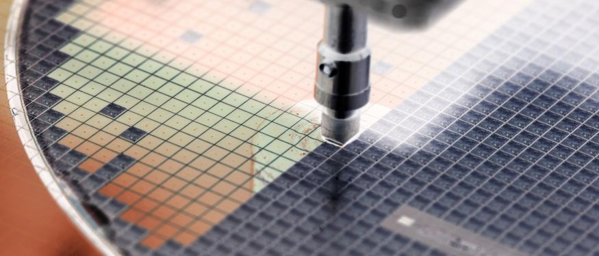
How Are Semiconductor Wafers Made?
Semiconductor wafers are made through a process called the Czochralski method. This begins with a single seed crystal which is inserted and spun in a large crucible. The process is repeated continuously until a large single crystal of silicon along with the doped atoms of the conductive metal weighing several hundred pounds is formed. The crystal is then tested for purity. Once approved, it is shaved into thin slices and buffed to remove any impurities.
What Are Semiconductor Wafers Used For?
A wafer in semiconductor manufacturing is one of the most versatile tools. In theory, semiconductor wafers are the blank sheet of paper used in the electronics industry. A semiconductor wafer can take anything added to it for use.
The most common use for semiconductor wafers is in the manufacture of microchips. These chips, like the wafers, are so linked with the substance they’re made of that the term silicon chip is commonly used. Furthermore, the region most commonly associated with computer chips is known as “silicon valley.” The wafers are prized for their conductivity and ability to store information.
Another, increasingly prominent use of semiconductor wafers is in the field of solar cells. With their high responsiveness to light, semiconductor wafers are an ideal medium for the production of photovoltaic cells. As the solar power industry increases in popularity and technology improves, look to see this field expand.
Semiconductor wafers are also used in testing. With a test wafer, such work as product development, material screening, and demonstration of machines is possible. Test wafers are similar to standard or prime-grade wafers, but have a few variances. They aren’t as clean or flat and the standards for them are less rigorous.
The Future of Semiconductor Wafers
So, what are wafers and what are wafers used for? It’s important to look to the future of this essential technology. Wafers, like all technology, are constantly evolving. One of the most important areas in which semiconductor wafers are evolving is getting larger. While many other technologies have shrunk, semiconductor wafers have constantly grown from the original 1-inch wafers to today’s 300mm standard wafer. The next step is predicted to be a 450mm wafer which will more than double the yield of chips from a current wafer.
Wafers are also predicted to get thinner at the same time. While the wafers themselves need to get larger, the devices the chips go in continue to shrink. As semiconductor wafers are well suited for microcomputing, the chips shrinking in depth are a must to fit the increasingly small devices.
Finally, the critical element lying ahead for semiconductor wafers is simply a dramatic increase in demand. As every possible technology has increased demand for microprocessor chips amid demand for smart technology, semiconductor wafers will remain in the hot market. While increasing the size for increased yield will help, semiconductor wafers are likely to increase in production for the foreseeable future.
As a modest device, a thin sheet of silicon ideal for designing circuits or various patterns, the wafer might seem unimposing. But with a wide diversity of uses almost as limitless as the technology itself, the semiconductor wafer stands to remain the base for technology for years to come.
If you need a quality wafer, consider Silyb Wafer Services. We specialize in short-loop, patterned test wafers designed for planarizing or flattening wafers for the manufacturing of integrated circuits. Visit our site today to see what we can do for you.
Published June 22, 2023.