Did you know that test wafers have an important role? They help improve the performance of semiconductor manufacturing processes. They are vital in optimizing techniques like Chemical Mechanical Polishing (CMP) and etching.
Are you interested in learning more? Have you wondered, "What are test wafers?" If so, keep reading.
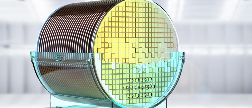
What Are Test Wafers?
It is important to note the semiconductor wafer design. Test wafers can be either blanket wafers or patterned wafers.
Blanket wafers are uniform and do not have any specific patterns. They can help engineers understand the performance of:
- Chemical Mechanical Polishing (CMP)
- Etching processes
Patterned wafers have specific designs or structures. These mimic the manufactured circuits or components.
These patterned test wafers aid in evaluating various aspects of the manufacturing process. Examples include lithography or deposition.
Benefits of Test Wafers
Using a test wafer in semiconductor manufacturing offers several benefits. With them, engineers can analyze the performance of different manufacturing steps.
This is possible without using expensive and time-consuming techniques on actual production wafers. This allows them to optimize processes, reduce defects, and enhance efficiency. Learn more about the benefits of text wafers here.
CMP Performance
One of the key benefits of test wafers is that they enable the assessment of CMP performance. CMP is a critical step in semiconductor manufacturing. It involves planarizing the wafer surface to ensure uniformity.
Engineers can fine-tune the process parameters. They do this by testing CMP performance on dedicated test wafers.
They can also reduce variations. This leads to better results on production wafers.
Etching Processes
Test wafers can also help determine if the etching process is efficient. Etching involves removing specific materials from the wafer to create patterns or features.
Test wafers allow engineers to experiment with different etching techniques. It also makes it possible to optimize them for the desired results.
Cost and Time Efficiency
Test wafers bring cost and time efficiency to semiconductor manufacturing. Engineers do not have to subject production wafers to extensive and expensive testing. Instead, engineers can use dedicated test wafers to analyze and fine-tune manufacturing processes.
This approach allows them to identify and rectify potential issues early on. It also helps reduce the defects risk and optimize production efficiency.
Improved Semiconductor Manufacturing
The semiconductor industry must continue to improve its products and technologies. One way to do this is by incorporating test wafers into manufacturing.
The insights from these evaluations are invaluable. They help engineers refine and enhance manufacturing steps. This results in higher-quality semiconductors.
This translates into better performance of electronic devices. Did you know that many electronic items you use daily rely on these semiconductors?
It's true. Some of the items include:
- Smartphones
- Computers
- Medical equipment
As a result, having the right processes and materials is essential. This is where semiconductor wafers come in.
Understanding the Role of Test Wafers
Have you wondered, "What are test wafers?" If so, you should have a better understanding now. They have an important role in semiconductor manufacturing.
When discussing test wafers, there's something important to remember. They are not used for probing or finished semiconductor testing.
Instead, they work to improve the performance of manufacturing processes. This includes CMP performance and etching techniques.
Do you have questions about test wafers? Do you want to learn more? If so, contact us.
Published June 22, 2023.