Chemical mechanical planarization is so complicated that it baffles even engineers and researchers.
In all fairness, the same is true of most components in modern electronics. So in this article, we break down a tiny element of modern manufacturing. You'll understand why planarization is so important in no time.
Just keep reading.
What is Chemical Mechanical Planarization (CMP)?
What is chemical mechanical planarization?
In (very) simple terms, it's about making surfaces flat and smooth. The process dates back to the 1950s. However, its importance grew a lot in the late 20th century.
Semiconductor devices were becoming widespread.
By the 1990s, it became necessary for flattening processes to become highly precise. Chemical mechanical planarization (CMP) has only gotten better since.
Also known as chemical mechanical polishing, CMP is the process of flattening a wafer for use in integrated circuits. CMP is used in the semiconductor and microelectronics industries.
It also has numerous applications in manufacturing. Wafer polishing and shallow trench isolation processing are two examples.
Chemical Mechanical Polishing vs. Chemical Mechanical Planarization
While the two terms are often used interchangeably, there's a subtle difference. Chemical mechanical polishing refers to the process of achieving a smooth surface by removing material.
Chemical mechanical planarization aims to create a flat surface by reducing variations in topography.
In spite of these differences, both terms describe a very similar process.
The Chemical Mechanical Planarization Process
The chemical mechanical planarization process involves five core steps from beginning to end:
- Wafer preparation
- Slurry application
- Polishing
- Monitoring
- Post-CMP cleaning
Wafer Preparation
Before CMP begins, the wafer must be prepared.
This involves cleaning its surface to remove contaminants. Particles, dust, and organic residues can all interfere with the process and have to be removed. Then, the wafer is mounted onto a carrier for the chemical mechanical planarization process.
Slurry Application
After preparation, a slurry is applied to the wafer surface. The slurry contains abrasive particles and reactive chemicals.
Typically, the particles are sub-micron-sized. The chemicals used in the slurry vary depending on the material being treated.
Both mechanical and chemical wafer polishing occurs through the application of the slurry.
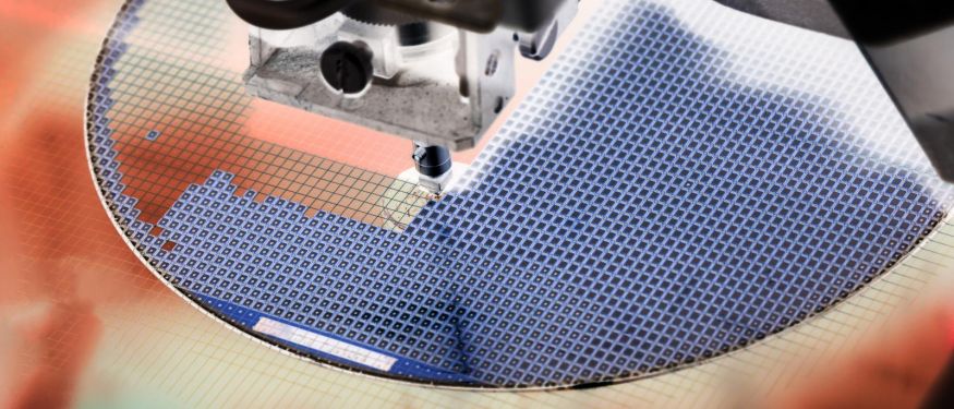
Polishing
A polishing pad made of polyurethane facilitates the planarization process. During polishing, the pad presses against the wafer and both are rotated. The resulting mechanical and chemical reactions flatten the wafer's surface and remove imperfections.
Monitoring
The CMP process must be carefully monitored to achieve the desired level of planarization. This is done by measuring the removal rate of the material and adjusting parameters along the way. Pressure, rotation speed, and slurry flow rate adapt as needed.
This is critical to ensure the process stops at the right time. Otherwise, damage to the wafer can result.
Post-CMP Cleaning
The final stage is to clean the polished wafer thoroughly.
This removes residual slurry and contaminants. This is typically done with brush scrubbing, high-pressure rinsing, and spin-drying.
Uses of CMP
What is chemical mechanical planarization used for?
Chemical mechanical planarization of microelectronic materials is used across various industries. Those include wafer polishing, damascene processing, and Shallow Trench Isolation (STI).
Wafer polishing is one of the primary applications of CMP. It's essential for ensuring smooth, flat surfaces on silicon and compound semiconductors. Damascene processing is a method of patterning metal interconnects in semiconductor devices.
In this process, CMP removes excess metals.
CMP is also widely used in STI. STI is essential for isolating active regions in semiconductor devices. It involves etching trenches and filling them with insulation.
In STI, CMP planarizes the insulating layers to ensure proper electrical isolation.
Other applications of CMP exist across the electronics industry. Some of them include:
- Hard drive manufacturing
- Optical component fabrication
- Three-dimensional integrated circuit (3DIC) packaging
Advantages of CMP
The chemical mechanical planarization of microelectronic materials offers several benefits. That's why it's so common across multiple industries.
CMP is versatile.
It's used to planarize a wide variety of materials. From different metals to silicon to oxide films, the process often uses the same setup. This can cut manufacturing costs significantly.
CMP is also environmentally friendly because it doesn't require the use of hazardous gases. When working with certain materials, CMP is also essential. For instance, CMP is the only viable way of patterning semiconductor devices when working with copper.
Finally, CMP allows for global planarization. This means it can planarize an entire wafer's surface at once. The result is a smooth, uniform surface across the material.
Future Trends in CMP
Modern electronic devices are at the cutting edge of innovation. As they continue to evolve, the demands on CMP processes will also increase. Some exciting developments in the industry include:
- Advanced materials
- Optimized processes
- Better environmental considerations
- New applications of CMP
The development of new materials will require CMP to adapt. High-K dielectrics and new barrier metals are two such examples.
As technology progresses, the demand for greater precision at lower costs goes up. That means more focus on improved equipment and process controls.
And concerns about the environmental impact of technology have also reached broader consideration. Increasing worries about semiconductor manufacturing will lead to a greater push for more sustainable practices.
Greener materials and processes are guaranteed to emerge.
Finally, CMP will continue to find new applications. That's thanks to its versatility and cost-effectiveness. Advanced display technologies, wafer-scale packaging, and alternative substrate materials are but three examples.
An Integral Part of Our Tech
Chemical mechanical planarization is a critical process in modern microelectronics. It enables the creation of ultra-smooth surfaces on a variety of materials.
And as devices continue to evolve, the importance of CMP will only grow.
At Silyb Wafers, we offer cutting-edge, patterned silicon wafers designed for CMP. We design our products with industry leader feedback to ensure ease of use and applicability across the industry. Click here to arrange a consultation with us.
Published June 21, 2023.